 CN
CN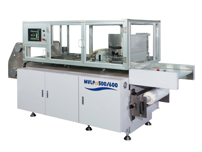

Quality Like Gold · Seek Perfection
Quality Like Gold · Seek Perfection
Everyone is searching.: PCB Equipment 、 IC Substrate Equipment 、 JSW Vacuum Laminator 、 Vacuum Leveling Machine
JSW Vacuum Laminating machine MVLP α 500/600
Vacuum lamination, UF lamination for TSV wafers, insulation layer formation for PCBs, cover layer for flexible substrates, rigid bonded boards, PCB, hole drilling, circuit patterning, circuit patterning for touch panels, lamination of insulating and sealing materials for various electrical appliances and electronic components, as well as thermal transfer of optical and fine patterns.
| MVLP α 500/600 | |
|---|---|
| Molding temperature | Max 180℃ |
| Forming pressure | Max 1.0Mpa |
| Molding size | 510*600*3mm |
| The vacuum level is reached in the hot plate | < 4hPa/15sec |
| Conveying speed | 60~180mm/sec |
| Conveying accuracy | ±1mm |
| Machine size | 3165*1310*1700mm |
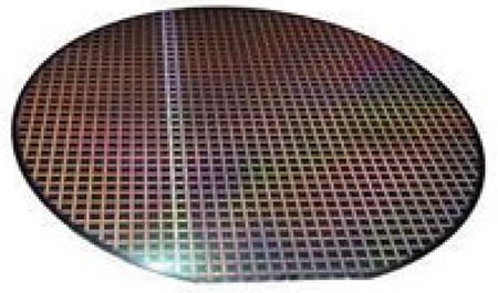
4~12 inch wafer5~8 inch Wafer ring +
WaferLamination for NCF
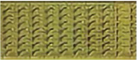
FPC
Lamination for DFR/DFSR/Pl film
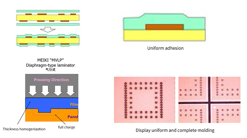
1.Fill the adhesive material into fine patterns under cacuum conditions.
2.It ensures no bubbles around the patterns,no wrinkles on the firm,and achieves uniform lamination.
3.The surface pressure application method ensure stronger dry firm adhesion,more uniform lamination pressure,and more consistent heat distribution on the dry firm.
4.It enables excellent lamination with uniform pressure applied over a wide range under vacuum conditions.
 Brand & Channel Advantage
 R&D & Production Advantage
 Industry Solution Advantage
 Global Service Advantage

Tel: 0769-26387119
Mobile: 158-0769-8576
Email: shiweiwei@cijinn.com
Address: Building F7, Tianan Digital Park, No.1
Huangjin Road, Dongguan City, Guangdong Province
Tel: 158-1826-6926
Contact: Ms. Mo
Email: molimin@cijinn.com
Address: Room 1507B, 15/F, Eastcore, 398 Kwun
Tong Road, Kwun Tong, Kowloon, Hong Kong
Tel: 158-1826-0792
Contact: Mr. Shi
Email: shiweiwei@cijinn.com
Address: Unit A, 16th Floor, Building A,
Bangna Tower, Samut Prakan, Bangkok

Douyin QR Code

Add WeChat Friend