 CN
CN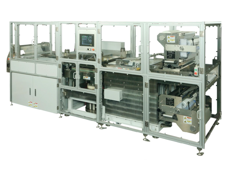

Quality Like Gold · Seek Perfection
Quality Like Gold · Seek Perfection
Everyone is searching.: PCB Equipment 、 IC Substrate Equipment 、 JSW Vacuum Laminator 、 Vacuum Leveling Machine
JSW Vacuum leveling machine MVLP500/600-IIW
The products are widely used in IC substrates, glass substrates, semiconductors and other industries, and the surface flatness of the products can reach a higher level through vacuum and flattening
1. Four languages are available: Japanese, English, Chinese, and Korean
2. Through segmented precision processes, continuous automated operations, and the synergy of carrier films, we enhance production efficiency while strengthening control over product quality.
3. The hot-pressing leveling steel plate features a mirror-finish surface. For its flatness, the test shows a maximum deviation of ≤10μm. For substrates with a thickness of 0.1mm–0.6mm and a step difference of 18μm, when the dry film ink thickness is 30μm, the ink thickness variation remains ≤5μm.
4. High-precision embeddability and high-precision flatness.
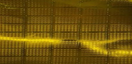
Unetreated Surface Effect
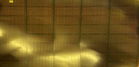
After Leveling Effect
| 1st Stage | |
|---|---|
| Parameter Name | Value |
| Forming Temperature | Max 180℃ |
| Forming Pressure | Max 1.0Mpa |
| Vacuum Degree | < 4hPa/15sec |
| 2nd Stage | |
| Forming Pressure | Max 2.0Mpa |
| Forming Temperature | Max 150℃ |
| Forming Size | 520×620mm |
| Sheet Flatness | Deviation ≤15μm |
| Conveying Speed | 60~130mm/sec |
| Conveying Accuracy | ±1mm |
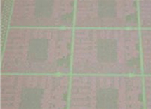
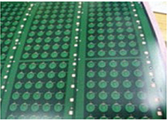
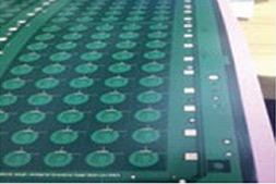
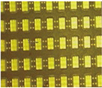
| Product Category | PCB board | Carrier board | Wafers |
|---|---|---|---|
| Icon |
|
|
 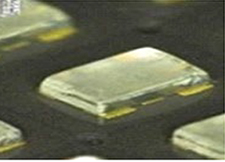
|
| Features | The line width and linespadng are less than2um/12um line width. | The line width and line spacing are narrow. The ink thickness uniformity is high. | The wafers are denseandhave alarge heightdifference. |
 Brand & Channel Advantage
 R&D & Production Advantage
 Industry Solution Advantage
 Global Service Advantage

Tel: 0769-26387119
Mobile: 158-0769-8576
Email: shiweiwei@cijinn.com
Address: Building F7, Tianan Digital Park, No.1
Huangjin Road, Dongguan City, Guangdong Province
Tel: 158-1826-6926
Contact: Ms. Mo
Email: molimin@cijinn.com
Address: Room 1507B, 15/F, Eastcore, 398 Kwun
Tong Road, Kwun Tong, Kowloon, Hong Kong
Tel: 158-1826-0792
Contact: Mr. Shi
Email: shiweiwei@cijinn.com
Address: Unit A, 16th Floor, Building A,
Bangna Tower, Samut Prakan, Bangkok

Douyin QR Code

Add WeChat Friend